The packaging of MEMS devices is one of the most challenging hurdle to MEMS commercialization. MEMS devices typically comprise of cavities, free-standing or even out-of-plane microstructures, which integrated circuits (ICs) do not have. Due to this major difference in nature between MEMS and IC, packaging for MEMS must allow space for actuator movement, let the sensing element be able to interact with the surroundings via a pathway, or provide a suitable ambient inside package to achieve higher sensitivity or better reliability. By adopting similar fabrication process flow and CMOS compatible materials such as Cu/Ni/Au metallization, such low temperature wafer bonding techniques also allows for 3D IC integration and extension of Moore's Law, hence creating a new generation of tiny but powerful devices.
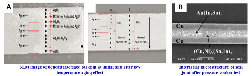
Low temperature fluxless solder for wafer bonding has received a lot of attention due to its great potential in hermetic MEMS packaging. Previous research activities deploy mainly solder alloy of eutectic composition to achieve low bonding temperature. In this project, we proposed new intermediate bonding layers (IBLs) of rich Ag composition in In–Ag materials systems. We investigated the intermetallic compounds (IMCs) at the bonding interface with respect to the bonding condition, post-bonding room temperature storage and post-bonding heat treatment. In addition, we have also conducted design, simulation and experimental development of wafer level vacuum packaged MEMS high speed scanning mirrors. We have also spent considerable effort on low temperature hermetic wafer bonding using In/Sn solder interlayer and Cu/Ni/Au metallization for MEMS packaging application, in which the thin Ni layer act as a buffer layer to control the diffusion process between solder interlayer and Cu. This technology can be adopted to build 3D ICs with the use of Cu vertical vias.
- Chengkuo Lee, Aibin Yu, Liling Yan, Haitao Wang, Johnny Han He, Qing Xin Zhang and John H. Lau, Characterization of intermediate In/Ag layers of low temperature fluxless solder based wafer bonding for MEMS packaging, Sensors and Actuators A., vol. 154, no.1, pp.85-91, 2009. [PDF] [DOI]
- Da-Quan Yu, Chengkuo Lee, Li Ling Yan, Meei Ling Thew, and John H. Lau, Characterization and Reliability Study of Low Temperature Hermetic Wafer Level Bonding Using In/Sn interlayer and Cu/Ni/Au Metallization, J. Alloys and Compounds, vol. 485, 1-2, pp.444-450, 2009. [PDF] [DOI]
- Da-Quan Yu, Chengkuo Lee, Li Ling Yan, Won Kyoung Choi, Aibin Yu and John H. Lau, The Role of Ni Buffer Layer on High Yield Low Temperature Hermetic Wafer Bonding Using In/Sn/Cu Metallization, Appl. Phys. Lett., vol. 94, 034105, 2009. [PDF] [DOI]
- Da-Quan Yu, Li Ling Yan, Chengkuo Lee, Won Kyoung Choi, Meei Ling Thew, Chin Keng Foo, and John H. Lau, Wafer-Level Hermetic Bonding using Sn/In and Cu/Ti/Au Metallization, IEEE Trans. on Components and Packaging Technol., vol. 32, no.4, 926-934, 2009. [PDF] [DOI]
- Riko I Made, Chee Lip Gan, Li Ling Yan, Aibin Yu, Seung Wook Yoon, John H. Lau, and Chengkuo Lee, Study of Low Temperature Thermocompression Bonding in Ag-In solder for Packaging Applications, J. of Electronic Materials, vol. 38, no.2, pp. 365-371, 2009. [PDF] [DOI]
<<< Back to Research Areas
Chengkuo Lee group
Electrical and Computer Engineering
National University of Singapore
4 Engineering Drive 3
Singapore, 117583
+65 6516-5865